You are here: Foswiki>DaqSlowControl Web>DaqUpgrade>DaqUpgradeOverview (2009-12-31, JanMichel)Edit Attach
DAQ Upgrade
This document gives an overview of why and how we want to upgrade our HADES-DAQ/Trigger-System. The upgrade at a glanceMotivation for an Upgrade
For light systems the DAQ shows approx. the following performance:| max. LVL1 | max. LVL2 | LVL2 Trigger downscaling factor | |
|---|---|---|---|
| pulser rate | 17kHz | 4-5kHz | 10-20 |
| in beam | 8kHz | 1 kHz | 10-20 |
| max. LVL1 | max. LVL2 | LVL2 Trigger downscaling factor | |
|---|---|---|---|
| in beam | 3-4kHz | 1-2 kHz | around 3 |
- The limitation of the LVL1 rate
- The main problem is the bad LVL2-Trigger reduction value
- Increase LVL2-rate capability
- Increase LVL1-rate capability
- Improve on the LVL2 trigger-algorithm
Upgrade Plans/Measures
The following measures are planned/performed:| measure | impact / aim | status |
|---|---|---|
| VME-Linux CPUs | LVL2 rate times 2-4 for MDC and Shower | done for all subsystems except RICH (2006-03-03) |
| TOF-readout and IPU | LVL1 rate of TOF system higher than 30 kHz | See below |
| MU + concentrator | LVL1 rate higher than 30 kHz | Marek can start in Summer 2006 on this, Hardware available |
| RICH FEE | LVL1 rate with data higher than 30 kHz, low noise in FEE | beg. 2007, Michael Bhmer, project till mid. 2008 |
| MDC readout | LVL1 rate > 30kHz + 5 MBytes/s / chamber | started end of 2006, MDC-Addon produced, under test |
| MDC cluster search (IPU) | ability to combine this information with RICH-IPU-rings | no timeschedule, could be started in March. 2007 |
| Compute Node for IPUs | "unlimited resources" for IPU algorithms | no timeschedule |
| Additional, new projects | ||
| RPC readout and Trigger | current LVL1 rate of TRB: 30kHz, LVL2 rate: 1kHz | working on this project since a year, new version: beg. 2007 |
| Forward Wall | approx. 300 channels, time and amplitude | EU-FP6 project, TRBv1, finished |
| Pion-Hodoscopes | approx. 200 channels | TRBv1, finished |
| Trigger-Bus | in combination with RPC-TRB | is currently developped in parallel to TRB2.0, TrbNet |
| Additional Projecs, LVL1 trigger | ||
|---|---|---|
| LVL1 trigger enhancment + consolidation with VULOM module | possibility for more debugging and better LVL1 trigger | M.Kajet. + Davide Leoni, finished in April 2007 |
- RPC-Wall
- Pion-Hodoscopes
- Forward-Wall
- MDC readout and hit-finder (without the TDCs on the board)
- TOF system, if the FEE of TOF will be exchanged
- RICH-FEE-readout and Readout-Controller-Functionality (Mnchen agreed on that)
- For the PANDA gas-chambers
- For the CBM-Mimosa readout for Frankfurt
- ....
Architecture of new DAQ/Trigger-System
Here I want to show the future architecture of the DAQ-System as discussed in our DAQ-Meeting 2006-02-28. Most important: The upgrade will be done in a way, so that the whole old system can stay as it is. The will be no time, where we have to change electronics in all subsystems at once, we want to try to do it step by step.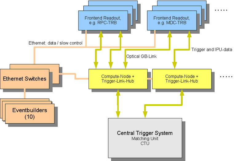 The key components are the following:
- In the end we will only use TRBv2 platform modules with detector dependent Addon-boards for the readout of the FEE, LVL1 and LVL2 pipes. This is one main point we learned from the past times: The zoo of different hardware made the maintainance quite complicated and manpower-intensive.
- Data transport is done by Ethernet. No VME-System is needed anymore.
- TDC/ADC and readout moves to the FEE. No long cables from the detector to the TDC.
- We have a tree structure of the Trigger-System, only point to point links, realized with GB-optical links.
- The same link will be used for IPU-data transport and so for the LVL2 trigger.
- The Trigger-Hubs are just a piece of code in a hardware which is a general purpose compute-node.
More detailed Architecture
The full DAQ system will consist of- 24 TRBv2 for RPC (LVL2 trigger implemented on DSP on TRBv2)
- 12 TRBv2 for MDC
- 12 TRBv2 for TOF
- 6 or 12 RICH-TRBv2
- 6 TRBv2 for Shower-Readout
- 3 TRB for Forward-Wall
- 4 TRB for Pion-Hodoscopes
Datarates
In the case we have no LVL2 trigger system running in the beginning of 2009 (heavy ion beam year!) we can expect the following data rates for Au+Au:20kHz LVL1:
| System | Max. Data-Rate in MBytes/s in spill | comment |
|---|---|---|
| MDC | 134 | ((37 * 8 * 2 * 20 000 * 6 * 2) / 1 024) / 1 024 = 134 |
| RPC | 32 | ((2 100 * 0.2 * 20 000 * 4) / 1 024) / 1 024 = 32 |
| TOF | 16 | ((700 * .3 * 20 000 * 4) / 1 024) / 1 024 = 16 |
| RICH | 110 | ((29 000 * 0.05 * 4 * 20 000 ) / 1 024) / 1 024 = 110 |
| Shower | 62 | ((30 * 30 * 3 * 0.1 * 2 * 20 000 * 6) / 1 024) / 1 024 = 62 |
Acromag module
The acromag module is an add-on PMC card for VME-CPUs. It will serve as the root-VME interface to the trbnet in the central trigger system. It could serve as well as an intermediate solution to read out the CEAN TDCs, and to read out standard VME modules on a longer timescale (the SIS scaler, latches, whatever). The acromag module will be connected with a 32-line LVDS cable to the hadcom module or the GP-Addon, and the trbnet protocol will be used for this cable. This was also one purpose to design the trbnet, since it will be independent from the medium it will be reused for the optical link. Status: VHDL code ready, simulated on the P2P connection (so no network/routing part up to now). First test are ongong with hardware (C. Schrader, J. Michel) in FrankfurtTRB
The TRB is developed and build in the frame of the EU-FP6-contract. This is the official task of Piotr Salabura. There is a large team working on it and we have a tight schedule to fulfill. Please have a look further down for the time-schedule. This also includes the integration of the optical GB-Transceiver to transport triggers and IPU-data to the Matching Unit (MU)MU_V2 / MU Concentrator / Trigger-System
Marek Palka will start working on this issue beginning in Summer 2006. The hardware with the optical links and powerfull DSPs is already available since over a year. It is just PLD- and DSP-programmingSome documentation about the MU V2 / concentrator is available here: http://www-linux.gsi.de/~michael/mu2_concept5.pdf The second possibility is to use a VME-CPU with the Acromag-PCI-Card to be used as the MU. The VHDL-code for the link-layer of the trigger-protocol is written by Ingo.
Compute Node
Wolfgang Khn proposed to use a compute node, which will be developed in Gieen. It is a very versatile module. It consists of an array of FPGAs, with a set of IO capabilities. The following picture show a block-diagram of what was intended to be built in Giessen: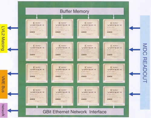
- array of 4-16 FPGAs
- Gigabit-Ethernet connectors (how many?)
- parts of the FPGAs have a PowerPC-Processor included
- optical links using the Xilinx-propritary MGTs
- memory
IPU/Trigger-Link
The only hard requirement we have to fulfill to include such a Compute-Node into the proposed Trigger-Scheme is the use of an optical GB-Transceiver at a transfer speed of 2 GBit. Industry standard is SFP: for example 2GBit: V23818_K305_B57 from Infineon (you can get these things from approx. 20 vendors). We use now: FTLF8519P2BNL (35/piece) The link-layer protocol we want to use has some limits imposed by the SerDes-Chips on the TRB. The current choice is the TLK2501 from TI. It is a 1.5 to 2.5 Gbps Transceiver and can directly be connected to the SFP-Transceiver. It uses a 8B/10B encoding to transmit data, but the user uses it just as a 16-bit FIFO, which means that we are limited to a wordlength which has to be a multiple of 16 bits (not really a limit). The TrbNet is the protocol layer used (see below). This protocol (VHDL-code and support) is provided by Ingo Frhlich and Jan Michel.TRB Architechture
Results from first experiments with the TRB can be found in the GSI Report 2005 or here: http://www-linux.gsi.de/~michael/GSI_2005_TRB.pdf The TRB V1.0 only has a readout function, no IPU data-path. The block-diagram is shown here: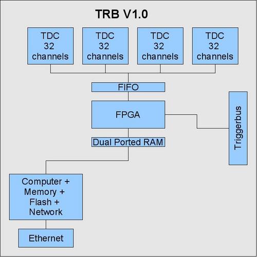 As there is no IPU link, the next version of the TRB has the following block diagram.
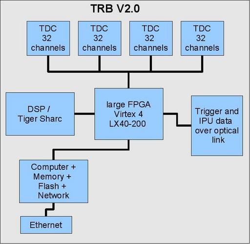
Main features of TRB V2.0
Large FPGA
Due to the demand of many pins and the possibility to use the FPGA for the algorithm, we have chosen a Virtex 4 LX40 with 768 user I/Os, 96*18kBit block RAM, 55k slices. Price: 430.DSP
The DSP will give us the possibility to have a very straight-forward and fast port of the existing TOF-algorithm to the RPC. For other systems, there is no need to put it on the board. The costs are around 150/piece. We want to use the TigerSharc DSP. Readout Processor We want to use a faster readout processor: ETRAX FS. Approx. 3 times faster than the Etrax MCM.Time Schedule for TRB 2.0
(estimated realtime time-schedules, not worktime) Due to many different delays, we are at least 6 month behind the schedule (2007-02-02):- ongoing tests with TRBv2a: DSP still under test.
- 15. February: submit the updated layout which will be called TRBv2b
- 15. March: tests with TRBv2b
- 15. April: Main functionality is given, same as TRB V1.0
- August: Fished implementation of TOF-algorithm in DSP and link to MU in Frankfurt by Ingo
Trigger-Bus-Architechture / IPU-Data paths
The motivation:- scalability: the current trigger-bus is not scalable, as we can not connect many systems to it. Maximum distance approx. 50 m and ground-shift problems are topics.
- maintainability/reliability: experience has shown, that the current cable connections are not reliable, cables are too big and heavy, very expensive, not easy to extend.
RICH readout architecture
The motivation: The current readout system based on GASSIPLEX chips is limited mainly by the readout controllers and the parallel TTL bus connection between the FEs and the RCs. Moreover, the current IPU hardware is also limited, especially in the case of direct particle hits in the MWPCs, and a higher number of noise pads in the RICH. The possibility to feed a new IPU with "grey scale" pictures instead of black-and-white ones as now would help in the case of direct particle hits, while a better noise reduction in the FEs would help in the latter case.A possible solution
First solution under discussion was to replace the RCs by TRBs with a RICH specific addon board, and to connect the 16 backplanes per sector by single LVDS links based on an ALTERA proprietary serial link protocol (which is available for free from ALTERA for educational applications). There would have been several critical points in this design:- crossing the abbyss between "technique of the last century" (i.e. 5V FEs) and a modern low voltage FPGA on the backplane
- still having to design with schematic based tools for the FE FPGAs (XC4005E), based on a ViewLogic license
- creating 16 different backplanes with fBGA packages
- maintaining another proprietary protocol (including error reporting, slow control, ...)
- still living with "old" GASSIPLEX preamps and their limitations
- (to be continued)
A hopefully better solution (the DPG2007 ansatz)
During DPG2007 in Giessen several people did meet and discuss another solution, based on an idea of Michael Bhmer, with important proposals from Michael Traxler and Ingo Frhlich. We concluded before DPG2007 that man power for the HADES DAQ upgrade is too precious to be spent in too many different projects, so we should use common work whereever possible. Another conclusion was to get rid of proprietary bus systems in the new DAQ system, to allow easy maintanance and debugging / error reporting / error tracing during development and operation of the system. Moreover, the re-usage of the work done by Ingo Frhlich in the new trigger bus allows to concentrate on a new frontend for the RICH, which should also be useful for other detectors (Si, MWPCs, CVDs) and / or experiments (FAIR). Please note: This design approach is the basis for discussion, and not yet settled! The new system will consist of several modules, as listed below:- analog frontend card (AFE)
- ADC card (ADC)
- passive backplanes (BP)
- logic module (LM)
RICH-FEE, APV25 and more
More information can be found here: RichFEEandDAQUpgrade.Debug data block
More information can be found here: DaqUpgradeSubEventDebugBlock.Advanced debug data block
More information can be found here: DaqUpgradeSubEventAdvancedDebugBlock. -- Michael Boehmer - 2007-03-20Parallel Event Building
- parallel Event Building scheme:
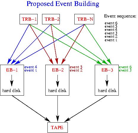
- Synchronous file writing. Synchronization is guaranteed by calibration events. The EB will stop writing current file and start new file when the following condition is fulfilled: currentEvent == calibrationEvent && number of collected events > some_number
- a second way to ensure synchronization: The CTS (Central Trigger System) sends special triggers which will set some bit in the data-stream, so that all eventbuilders close their files at the same time. [we have to think about some way to resynchronize when escpecially this event is lost in one event-builder.]
- Common run ID with timestamp. Common run ID will be distributed to all Event Builders in every sub-event together with trigger tag.
- Run information will be inserted into Oracle data-base by a script running on EB-1 machine. Start and stop times will be the times of the file from EB-1 and they will be identical for all other Event Builders. Run IDs will be unique for each file as well as the file names. Currently we are thinking about two types of run IDs: a) runID = commonRunID + EB_number, [this might introduce a dead time of 10 sec in case of 10 EBs], b) run ID consists of two numbers: commonRunID and EB_number.
- Synchronization of EBs is not obvious. One more idea would be to synchronize via a wall clock. However one has still to think about common run IDs.
- Estimate of the data rate in Au-Au collisions is about 200 MB/s. It has two impacts:
- We have 1 Gbit optical line which can transport only 100 MB/s to a data mover at a tape robot side. Thus we will need to install 10 Gbit slot and 10 Gbit fibre-optic cable.
- At the moment there are only 4 tape drives (with a speed of 80 MB/s each) which means theoretically 320 MB/s in total. IT department plans to buy two more tape drives which will increase a total till 480 MB/s. This still means that for the beam time almost all robots will be required to serve Hades. The maximum number of tape drives foreseen in the GSI mass storage system is 8/10.
- Some info: GSI mass storage system will be upgraded with IBM TotalStorage 3494 Tape Library with a capacity of 1.6 PBytes.
- Prices: 700 GB tape = 130 euro, tape drive = 20000 euro.
| I | Attachment | Action | Size | Date | Who | Comment |
|---|---|---|---|---|---|---|
| |
net.jpg | manage | 105 K | 2009-01-14 - 22:48 | SergeyYurevich | network structure |
| |
net_corr_cut.jpg | manage | 117 K | 2009-01-14 - 23:09 | SergeyYurevich | network structure |
| |
net_cut.jpg | manage | 127 K | 2009-01-14 - 23:31 | SergeyYurevich | network structure |
Edit | Attach | Print version | History: r33 < r32 < r31 < r30 | Backlinks | View wiki text | Edit wiki text | More topic actions
Topic revision: r33 - 2009-12-31, JanMichel
Copyright © by the contributing authors. All material on this collaboration platform is the property of the contributing authors.
Ideas, requests, problems regarding Foswiki Send feedback | Imprint | Privacy Policy (in German)
Ideas, requests, problems regarding Foswiki Send feedback | Imprint | Privacy Policy (in German)


