You are here: Foswiki>DaqSlowControl Web>DaqUpgrade>DaqUpgradeMDCOverview>MDCDevelopmentAndTesting>HardwareTest (2009-10-27, JanMichel)Edit Attach
MDC-Upgrade: MDC-Optical-Endpoint Hardware test
Here we collect the documents relative hardware measurementChip's temperatures
-- AttilioTarantola and Yanyu - 23 May 2008 In the attached document we record the temperature of the chips. The test's conditions are described in the document. The Lattice-device utilization during the test is:Ignore Preference Error(s): True
Device utilization summary:
APIO 4/18 22% used
PIO 13/330 3% used
13/140 9% bonded
IOLOGIC 2/330 <1% used
SLICE 102/9612 1% used
EBR 2/66 3% used
PLL 2/2 100% used
PCS 1/1 100% used
Number of Signals: 403
Number of Connections: 891
Pin Constraint Summary:
13 out of 13 pins locked (100% locked).
- chip_temperature.pdf: chip temperature
Level adapters: U1, U2, U3
-- AttilioTarantola and Yanyu - 23 May 2008 Introduction: the voltage translators U1, U2, U3 translate 5V<->3.3V. The stay in between the Lattice and the CLPD on the MB. In the picture: - yellow signal: clk (50 MHz) produced in the lattice. Input for U2 (pin 1), 2.6V. - green signal: output for U2(pin 20), 4.2V The time difference between the two signals is 3.1 ns. Enlarging the picture one can see the ground line stays 1V below the signal's minima (1,2) * U2 I/O print_000.jpg: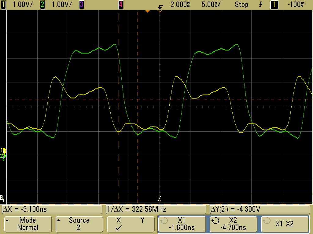 In the following pictures:
- yellow DRA: clk (50 MHz) produced in the lattice.
Input for U3 (pin 9).
- green signal: output for U3 (pin 20).
* U3 I/O print_001.jpg:
 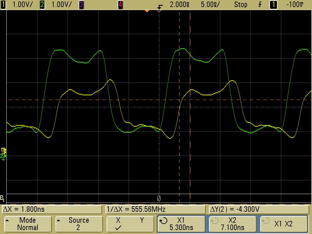 The time difference between the two signals is 1.8 ns
* U3 I/O print_002.jpg:
 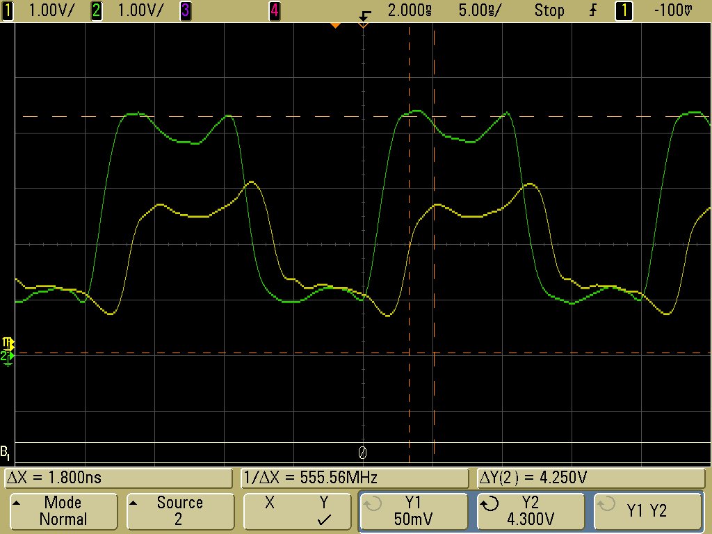 We didn't observe strange behaviors of U1,U2,U3.
They are always pretty warm and the temperature changes as described in the previous document (it depends of the I/O in use). Even with fast signals (clk 50 MHz) the output is present and delayed by few ns.
In the real case the fastest signal which will pass through the level adapter will be DST (data strobe 1-10 MHz).
Jitter measurement
06 Jun 2008 Differential measurement of the 100 MHz CLK (Silicon Lab 531BA135M000BG) jitter. The probe was connected at R1. -Number of acquisition:2000 -Statistical mean: 10 ns -Std. deviation: 5.7 ps In the following picture we probe the CLK signal at CS1: common stop pins. The CLK signal is generated by the CLK (Silicon Lab), it passes through the Lattice and then to CS1 -Number of acquisition:2000 -Statistical mean: 10 ns -Std. deviation: 7 ps -Pk-Pk:.50.87 ps The CLK has been divided by 8 and multiplied by 8. * MDC_100_MHz_PLL_1_to_1.jpg :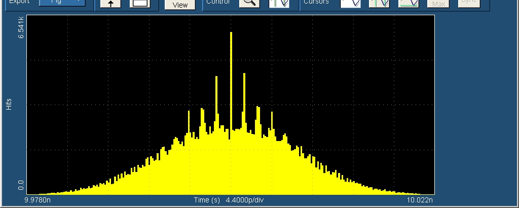 Following picture:The CLK has been divided by 5 and multiplied by 4.
-Number of acquisition:2000
-Statistical mean:(80 MHz)
-Std. deviation: 9.5 ps
-Pk-Pk: 80 ps
* MDC_100_MHz_times_4_div_5_hist.jpg :
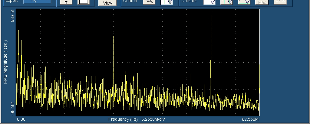
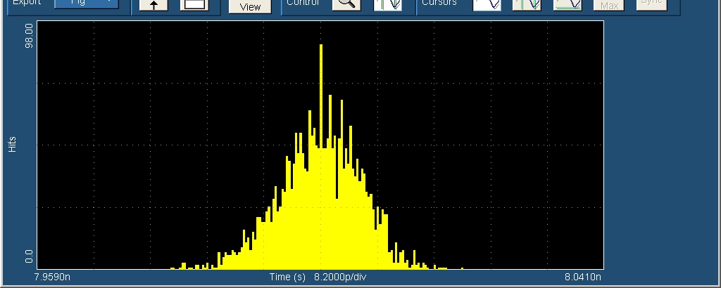
 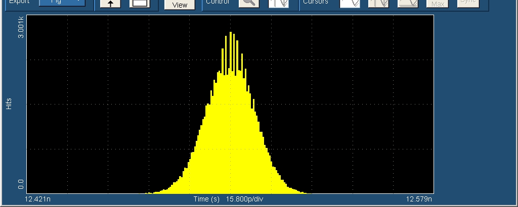 Following picture:The CLK has been divided by 4 and multiplied by 5.
-Number of acquisition:2500
-Statistical mean: 8 ns (125 MHz)
-Std. deviation: 7 ps - 6 ps
-Pk-Pk: 53 ps
* MDC_100_MHz_times_5_div_4_fft.jpg:
  * MDC_100_MHz_times_5_div_4_hist.jpg:
| I | Attachment | Action | Size | Date | Who | Comment |
|---|---|---|---|---|---|---|
| |
MDC_100_MHz_PLL_1_to_1.jpg | manage | 103 K | 2008-06-06 - 21:59 | AttilioTarantola | jitter 1 to 1 |
| |
MDC_100_MHz_PLL_1_to_1.png | manage | 9 K | 2008-06-06 - 21:57 | AttilioTarantola | jitter 1 to 1 |
| |
MDC_100_MHz_times_4_div_5_hist.jpg | manage | 92 K | 2008-06-06 - 22:08 | AttilioTarantola | CLK times 4 divided by 5 |
| |
MDC_100_MHz_times_5_div_4_fft.jpg | manage | 160 K | 2008-06-06 - 22:09 | AttilioTarantola | CLK times 5 divided by 4 |
| |
MDC_100_MHz_times_5_div_4_hist.jpg | manage | 97 K | 2008-06-06 - 22:11 | AttilioTarantola | histo:. CLK times 5 divided by 4 |
| |
chip_temperature.pdf | manage | 35 K | 2008-06-06 - 21:06 | AttilioTarantola | chip temperature map |
| |
print_000.bmp | manage | 2 MB | 2008-06-06 - 21:09 | AttilioTarantola | level adapter |
| |
print_000.jpg | manage | 98 K | 2008-06-06 - 21:29 | AttilioTarantola | level adapter |
| |
print_001.jpg | manage | 96 K | 2008-06-06 - 21:19 | AttilioTarantola | u3 I/O |
| |
print_002.jpg | manage | 96 K | 2008-06-06 - 21:21 | AttilioTarantola | U3 I/O |
Edit | Attach | Print version | History: r2 < r1 | Backlinks | View wiki text | Edit wiki text | More topic actions
Topic revision: r2 - 2009-10-27, JanMichel
Copyright © by the contributing authors. All material on this collaboration platform is the property of the contributing authors.
Ideas, requests, problems regarding Foswiki Send feedback | Imprint | Privacy Policy (in German)
Ideas, requests, problems regarding Foswiki Send feedback | Imprint | Privacy Policy (in German)


