MDC-Upgrade: Cooperation with Yanyu Wang
Introduction
In the HADES-DAQ-Upgrade project the MDC-Upgrade is an essential part.
The expected data rates for heavy ion systems can not be handled any more
with the original MDC-DAQ.
A description of the concept of the DAQ-upgrade and the new DAQ-system can
be found at:
http://hades-wiki.gsi.de/cgi-bin/view/DaqSlowControl/DaqUpgradeOverview
The idea behind the MDC-upgrade is to simplify everything (get rid of
VME,PPC,SAM,ROC,DTU) and put everything on a common platform for the whole
HADES-DAQ system.
A short overview of the old and new MDC-DAQ can be found here:
http://hades-wiki.gsi.de/pub/DaqSlowControl/DaqUpgradeMDCOverview/MDC-setup.pdf
The TRBv2 (optionally without TDCs when only digital communication is needed,
like in the case of the MDC-DAQ) will serve as this platform.
To test the new readout-scheme one needs to connect the TRBv2 to the MDC-FEE
(driver cards on the motherboard). For this purpose a MDC-ADDONv1 card was
developped and is currently (2007-02-02) being programmed by Attilio
Tarantola.
As this board is just using RS484 drivers for the communication
the known problems will stay:
- crosstalk and "ringing" of the MDC-FEE due to copper cables squeezed between motherboards
- heat disspation
- missing possibility to reprogramm the motherboard-CPLD
- hassle with the chains of motherboards
Project definition
Therefore, the project was started to evaluate and build a prototype board for the TRBv2 -> MDC-Driver-Card -> Motherboard communication.
The idea is to use only optical transmission for the data
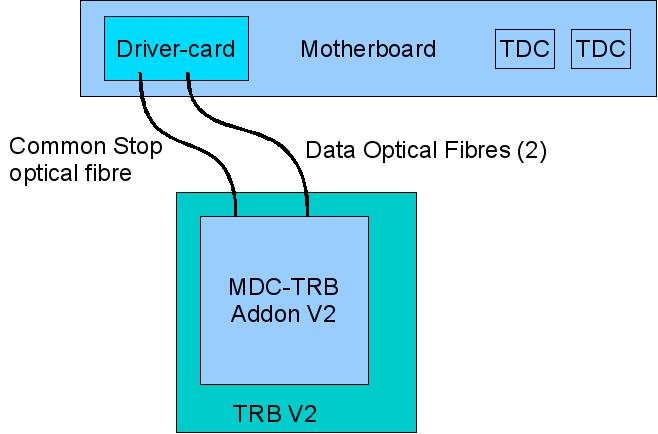
and the clock (only point-to-point connections). The data should be tranmitted via the optical transceivers and SERDES bidirectionally. Also the common or-signal can be transported via the data-stream (with high priority which is forseen in the TRB-Net protocol). Only the "Common-Stop" signal needs a good time resolution, so a dedicated optical transmitter has to be put on the driver-card and a receiver on the TRBv2-MDC-Addon_v2.
In total we need around 400 new driver cards (with FPGA).
The following picture illustrates the project. Each TRBv2-MDC-AddonV2 will have 32 optical transceivers as this is the maximum number of motherbaords for one MDC sector.
2008-05-19 It turned out in October 2007, that it is not possible to transmit a good timing signal via the cheap optical trasceivers.

More details about the project progess can be found
here.
--
AttilioTarantola - 16 May 2008
MB and DC Current measurement:
--
AttilioTarantola - 22 Apr 2008
Today Yanyu and me measured the MB+DC currents. We measured the following currents for long and short MB with all threshold fixed to 10. The calibration trigger was enabled such that we had one normal trigger and one calibration trigger. The Driver card were plugged onto the MB(as in normal operation): this means the TDCs, the CPLD and the 2 transceivers have the same common voltage +5VD.
| Motherboard |
Voltage |
Current(readout stopped) |
Current(readout running) |
| short |
+1V(green) |
150 mA |
160 mA |
| short |
-3.3V(yellow) |
-360 mA |
-360 mA |
| short |
+3.3V(orange) |
360 mA |
360 mA |
| short |
+5V(red) |
440 mA |
850 mA |
| long |
+1V(green) |
220 mA |
230 mA |
| long |
-3.3V(yellow) |
-520 mA |
-520 mA |
| long |
+3.3V(orange) |
510 mA |
510 mA |
| long |
+5V(red) |
540 mA |
700 mA |
Here the same measurement changing thresholds:
| Motherboard |
Threshold |
Dataword number(calibration) |
Dataword number(normal trigger-noise) |
Current relative +5V |
| short |
60 (all DBs) |
67 |
1 |
500mA |
| short |
10 (all DBs) |
67 |
52 |
850mA |
| |
| |
| long |
10 (all DBs) |
577 |
50 |
970mA |
| long |
60 (all DBs) |
not enabled |
2 |
970mA |
| |
| |
| long |
10 (all DBs) |
not enabled |
60 |
1,03A |
| long |
60 (all DBs) |
not enabled |
2 |
650mA |
| long |
10 (all DBs) |
530 |
60 |
1,03A |
We powered the MB(+5V,+3V,-3V,+1V) and the driver card (+5V) individually. Here the current relative +5V for the DC:
| Motherboard |
Threshold |
Current for DC(+5V)(readout stopped) |
Current for DC(+5V)(readout running) |
Dataword number(calibration) |
Dataword number(normal trigger-noise) |
| short |
10 (all DBs) |
250mA |
370mA |
67 |
40 |
| short |
60 (all DBs) |
|
260mA |
not enabled |
2 |
Here the current relative +5V for needed by the TDCs+CPLD:
| Motherboard |
Threshold |
Current for TDCs(+5V)(readout stopped) |
Current for TDCs(+5V)(readout running) |
Dataword number(calibration) |
Dataword number(normal trigger-noise) |
| short |
10 (all DBs) |
250mA |
370mA |
67 |
45 |
| short |
60 (all DBs) |
250mA |
250mA |
not enabled |
1 |
+5Volts study:
--
AttilioTarantola - 16 May 2008
14 May 2008 Yanyu and me tried to see the working mode of one short MB changing the +5V. The +5V(normal operating voltage for one short MB) is needed by the 8 TDCs, the CPLD and 2 transceivers.
The results are:
* Operating voltage (5V-4.7V): the readout is not affected by the voltage drop. This means we were able to get normal data (60 datawords per event) and calibration data (all channels calibrated). The MB worked as expected:no changes in DST (data strobe), AOD(address/data) and RDY(token back to Addon) signals.
* Operating voltage (4.4V): the event size for normal data does not change (60 datawords per event) but the data is always 0 and the calibration still is working fine (all channels calibrated). (Speaking with Joern, he suggested this behavior is due to the fact that the CMS does not reach the TDCs. At this operating voltage the TDCs should work without any problem and this we see in the calibration events where the common stop is not needed by TDCs).
No changes in DST(data strobe), AOD(address/data) and RDY(token back to Addon) signals.
Conclusion: the LDO, which Yanyu is looking for, might drop down to 4.85V. In this case the MB(TDC+CPLD) will not be affected.
--
AttilioTarantola - 04 Aug 2009
Jan and me: additional current measurement. Setup: 1 long MB, 2 DB stack, connected to 10 cm cable to a power
distributor board (v1 bridged). We read the current on the voltages power suppllies:
The voltages measured on the OEPB(input connector): 5.59V, 3.66V, 1.93V, +3.130V, -3.190V
OEPB(oputput LDO): 1.198V,3.342V, 1,000V, 5.007V,
On MB(TDC side): -3.17V,+3.10V
Long MB:
| Th |
*Nr.dataword |
I(+5V) |
I(3.5V) |
I(1.5V) |
I(3.0V) |
I(-3.0V) |
comment |
| before init |
- |
144 |
176 |
468 |
560 |
582 |
|
| x"00" |
- |
1440 |
176 |
472 |
568 |
580 |
|
LDO limit to 4.45V |
| x"05" |
- |
1440 @ 4.45V |
176 |
472 |
568 |
580 |
|
LDO limits reached, voltage dropping with time and temperature |
| x"10" |
100-120 |
1440 |
176 |
472 |
568 |
580 |
|
LDO limit to 4.45V |
| x"20" |
- |
668 |
176 |
472 |
568 |
558 |
|
| x"70" |
~10 |
550 |
176 |
472 |
568 |
580 |
|
Short MB:
| Th |
*Nr.dataword |
I(+5V) |
I(3.5V) |
I(1.5V) |
I(3.0V) |
I(-3.0V) |
comment |
| x"00" |
- |
1255 |
175 |
384 |
392 |
391 |
|
| x"10" |
- |
980 |
175 |
394 |
392 |
391 |
|
| x"20" |
- |
460 |
175 |
394 |
392 |
391 |
|
| x"30" |
- |
385 |
175 |
394 |
392 |
391 |
|
| x"40" |
- |
385 |
176 |
396 |
378 |
389 |
|
 More details about the project progess can be found here.
-- AttilioTarantola - 16 May 2008


