|
|
You are here: Foswiki>DaqSlowControl Web>TDCReadoutBoard>TDCReadoutBoardV3>ProposalAndFeaturesTRB3 (2012-05-07, JanMichel)Edit Attach
Layout Proposal (obsolete):
- TRB3_layout_proposal1.pdf: Layout proposal
- TRB3 updated layout:
Key Features
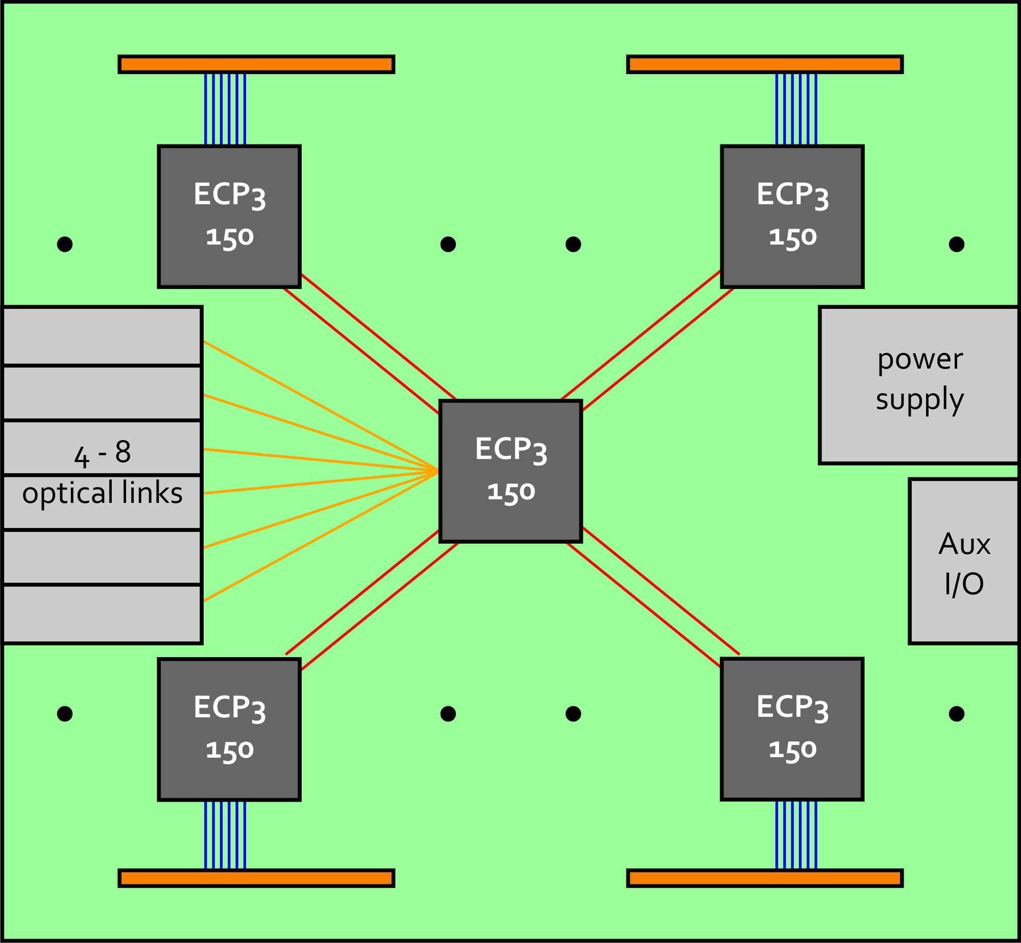
- 4 times LFE3-70E(A)-8FN672C for TDC (+ future applications, as e.g. ADC-readout )
- 1 central LFE3-150EA-8FN1156C
- smaller 48V power supply, based on Vicors BCM: http://cdn.vicorpower.com/documents/datasheets/BCM_48VFamily_DS.pdf, B048F060T24 is the type
- all other PoL regulators based on the Enpirion Products (evaluation board and devices are here at GSI): http://www.enpirion.com/products-en5396qi.htm or similar
- Add pads / holes around DCDC converters to replace them with an addon board (to use linear regulators in case the DCDC converters produce too much noise in analog data)
- 2 times 2 SFPs to the central FPGA: 2 for Ethernet and 2 for TRBNet (for example). The position is not really fixed as shown in the layout-proposal. Can be spread over the board.
clock
- Lattice Clock Manager is working for the FPGAs and SERDESes, http://www.latticesemi.com/products/ispclock/index.cfm?source=topnav (CLK5406 is used on the PEXOR3)
Connectors
- we leave the add-on connectors as they are on v2 controlled by the central FPGA.
- The connectors to each FPGA should be Samtec: QMS-104-09.75-L-D-A (mating part: QFS-104-06.25-L-D-A): Length 8,5cm These high speed connectors are similar to the AddOn connectors of the TRBv2, but are more rugged. They provide 208 pins + 3 power blades. Used by Jan Hoffmann and recommended by him.
- Standard reference time input: This then is fed to a fan-out chip, which will be fed to the FPGAs (twice as Marek said). And a RJ45 as secondary reference time input. (The input of the fanout-chips can select between two inputs. This can be done via a jumper.)
- Additional auxilary connectors, like RJ45 + a normal pitch pin-header, all connected to the central FPGA. *Many LEDs! (Please label them LED1..8, not dgood, dwait etc.) maybe 4 for each FPGA. And a test connector for each of the 4 FPGAs.
Connection between FPGA:
- SERDES connections
- Each of the TDC-FPGAs has two SERDES connections to the central FPGA, coming from two QUADS. If possible, put one line of one quad to the mini-addon-connector. Put a set of 12 LVCMOS25 lines between the central FPGA and each of the other FPGAs
- Each FPGA gets a FLASH to boot from.
- JTAG chain.
- DDR2-3 RAM and SRAM I would skip on the 4 FPGAs, I don't see the obvious application.
- Maybe an SRAM on the central FPGA. DDR3 is tricky and not !
- Two bit coding input to select the FPGA number - like on the MDC Hub2
Manpower
- Marcin: schematics: started on 2011-02-07
- Pinout definition: all, please help
- Greg can start with the UDP-communication protocol, replacing the ETRAX by a PC: start 2011-02-14
- Layout and production: Peter and Michael
- TRBNet implementation: Jan
- TDC-implementation: Cahit + Eugen
- TDC-Data-analyis, feature check etc.: Marek
Edit | Attach | Print version | History: r1 | Backlinks | View wiki text | Edit wiki text | More topic actions
Topic revision: r1 - 2012-05-07, JanMichel
Copyright © by the contributing authors. All material on this collaboration platform is the property of the contributing authors.
Ideas, requests, problems regarding Foswiki Send feedback | Imprint | Privacy Policy (in German)
Ideas, requests, problems regarding Foswiki Send feedback | Imprint | Privacy Policy (in German)