You are here: Foswiki>DaqSlowControl Web>TDCReadoutBoard>TDCReadoutBoardV2>TRBAddOns (2009-10-27, JanMichel)Edit Attach
Here we describe our various AddOn Cards for the TRBv2
HUB-AddOn
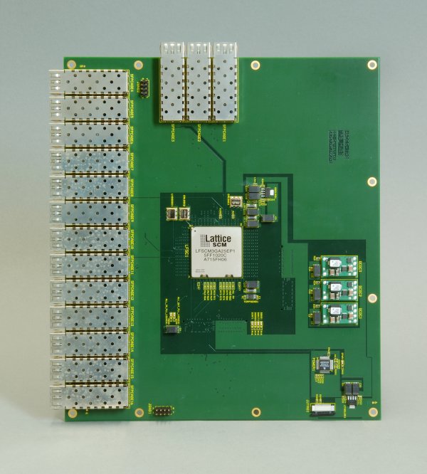
The TRB-HUB servers as the trigger fanout-module.It has 16 times a 2-GBit/s SFP. The SERDESes are in the LatticeSCM40 FPGA.
Fully impedance matched 12-layer PCB.

ShowerAddOn
The features of the ShowerAddOn alias General-Purpose-ADC-AddOn- 96 channels 10-bit ADCs
- 40/60 MSPS
- ADC type: AD9212 from Analog Devices
- low noise, variable gain amplifier at the input (AD8334 from Analog Devices)
- input voltage range: 275 mV (AC coupled),
- -3 dB bandwidth: 100 MHz (independent on gain)
- amplifier noise: 0.74 nV/sqrt(Hz), 2.5 pA/sqrt(Hz)
- Two 68-pin connectors, each connector contains:
- 48 analog inputs,
- 5 LVDS lines (programmable direction)
- 2 TTL lines (programmable direction)
- +5V (2 pins), GND (6 pins).
- Connector type: HDRA-EC68LFDT-SL from Honda Connectors
The General Purpose Add on: Short Description
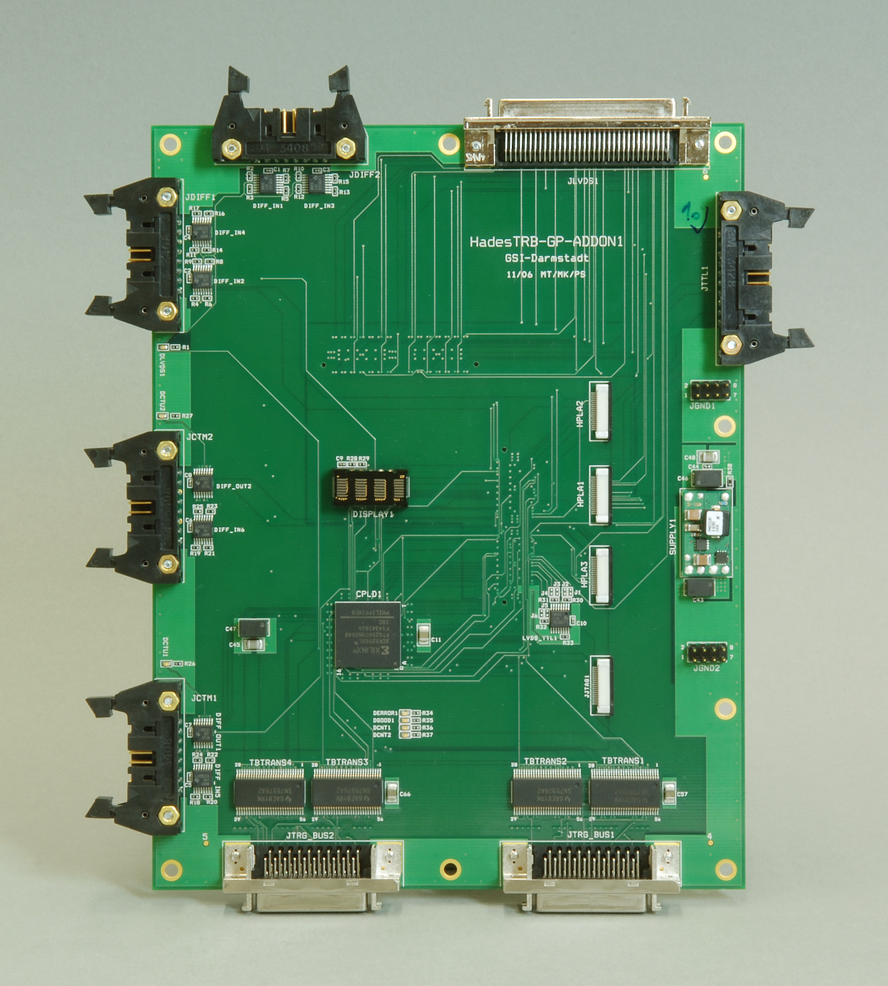
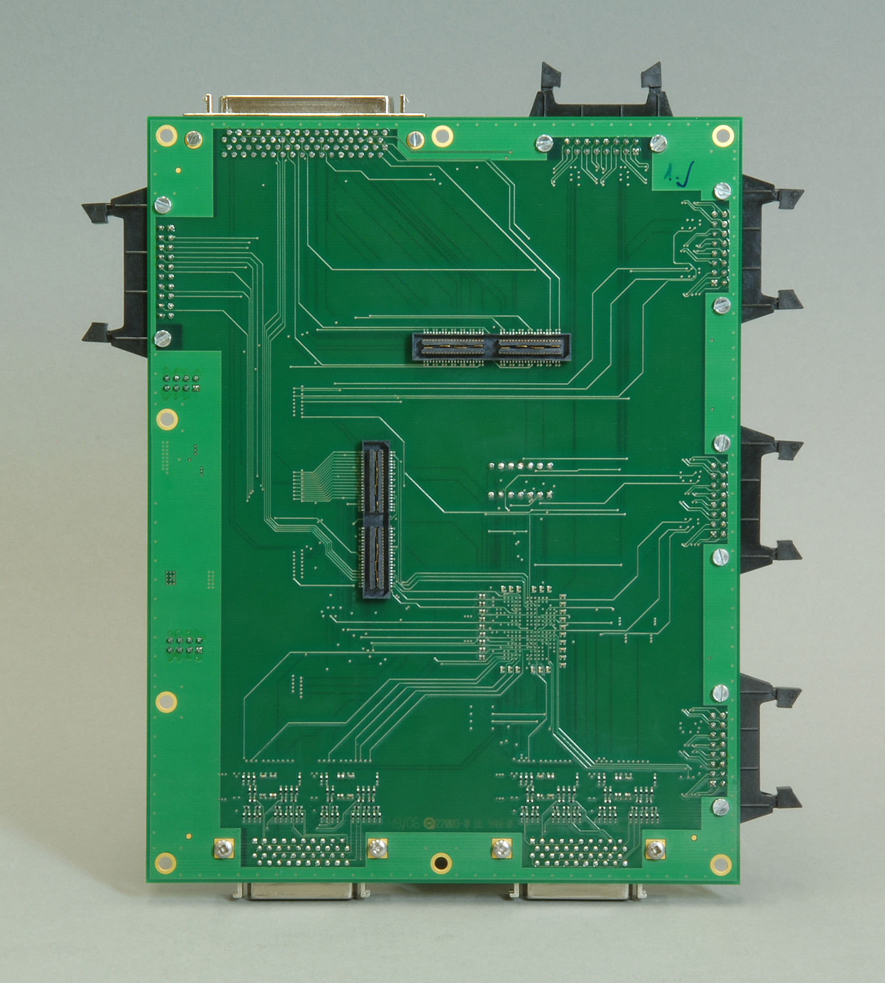
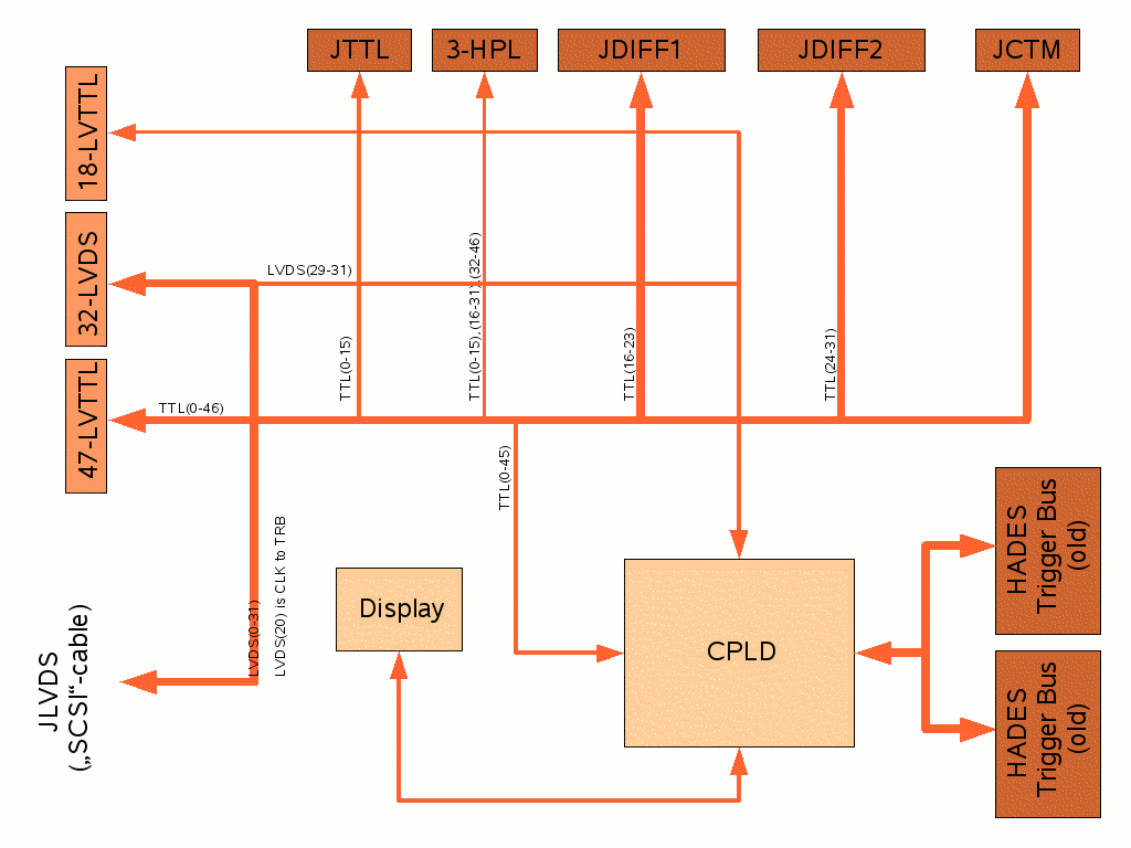
The General Purpose Add on (GP-AddOn) board povides the interface between the TRBv2 (main readout board) and many different signals. For example it can used as interface to the old HADES trigger bus. The GP-AddOn can be easily connected to the TRBv2 board through 2 connectors (QSE-040-01) placed on the back side of the board. The power supply is given to the GP-Addon through the connector's pins. A programmable logic CPLD ( XCR3128XL7VQ100C) is placed on the right hand side and is supported by Xilinx Web-PACK and industry standard CAE tools (Cadence/OrCAD, Exemplar Logic, Mentor, Synopsys, Viewlogic, and Synplicity), using HDL editors with ABEL, VHDL, and Verilog. Design verification uses industry standard simulators for functional and timing simulation. Here we attach the data sheets for further details of the board's component: General Purpose addon board: front view General Purpose addon board: back view
  General Purpose addon board: block diagram
Pinouts and connectors
- Pinout of the TRB-connectors and the AddOn-cards: TrbV2ConnectorsPinout
| I | Attachment | Action | Size | Date | Who | Comment |
|---|---|---|---|---|---|---|
| |
TRB_HUB1.jpg | manage | 2 MB | 2007-10-23 - 14:29 | MichaelTraxler | TRB-HUB1 |
| |
TRB_HUB1_small.jpg | manage | 64 K | 2007-10-23 - 14:34 | MichaelTraxler | TRB_HUB1 (small) |
| |
general_porpouse_addon.gif | manage | 56 K | 2007-07-23 - 17:47 | AttilioTarantola | general porpouse addon block diagram |
| |
gp_addon_back.jpg | manage | 2 MB | 2007-07-25 - 21:51 | AttilioTarantola | GP-AddOn back |
| |
gp_addon_front.jpg | manage | 2 MB | 2007-07-13 - 14:56 | AttilioTarantola | General purpose addon board |
Edit | Attach | Print version | History: r22 < r21 < r20 < r19 | Backlinks | View wiki text | Edit wiki text | More topic actions
Topic revision: r22 - 2009-10-27, JanMichel
Copyright © by the contributing authors. All material on this collaboration platform is the property of the contributing authors.
Ideas, requests, problems regarding Foswiki Send feedback | Imprint | Privacy Policy (in German)
Ideas, requests, problems regarding Foswiki Send feedback | Imprint | Privacy Policy (in German)


