|
|
You are here: Foswiki>DaqSlowControl Web>TDCReadoutBoard>TDCReadoutBoardV2>TRBBoardErrors>TrbPatches (2009-10-27, JanMichel)Edit Attach
AddOns
The pictures shown are a sized down. Download the file from the table to see the high resolution version.Trb2 B
Connect Temperature Sensor to FPGA: Via one data line from temperature sensor to pin AK17 / JT266 of FPGA. (This is the outermost testpad in a row of four next to C673. The Via is the uppermost in a group of three in a triangle form.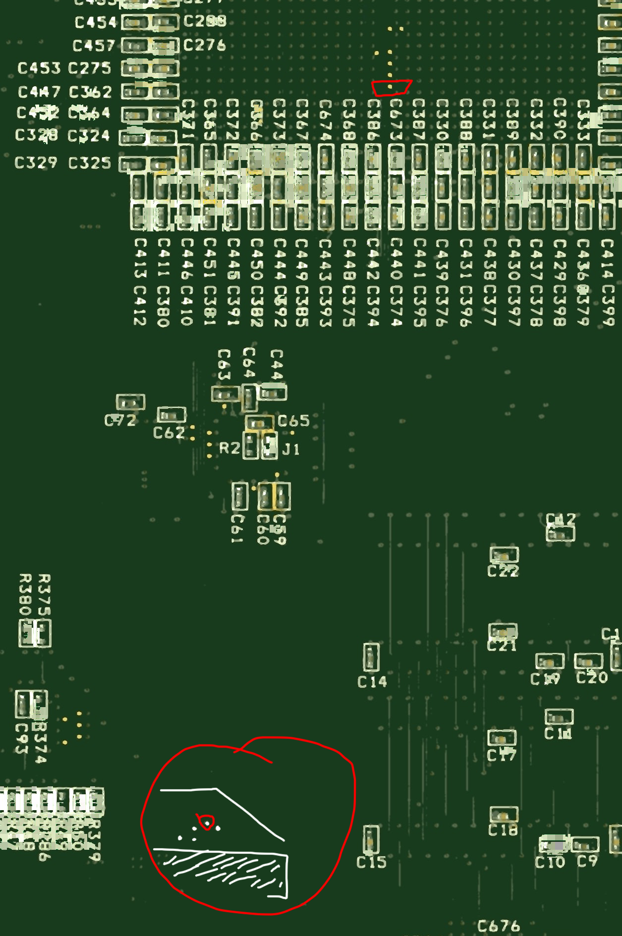
Trb2 C
Connect Temperature Sensor to FPGA: Via on data line from temperature sensor to pin AK17 / JT266 of FPGA. (This is the outermost testpad in a row of four next to C673. The Via is the single one right of R45.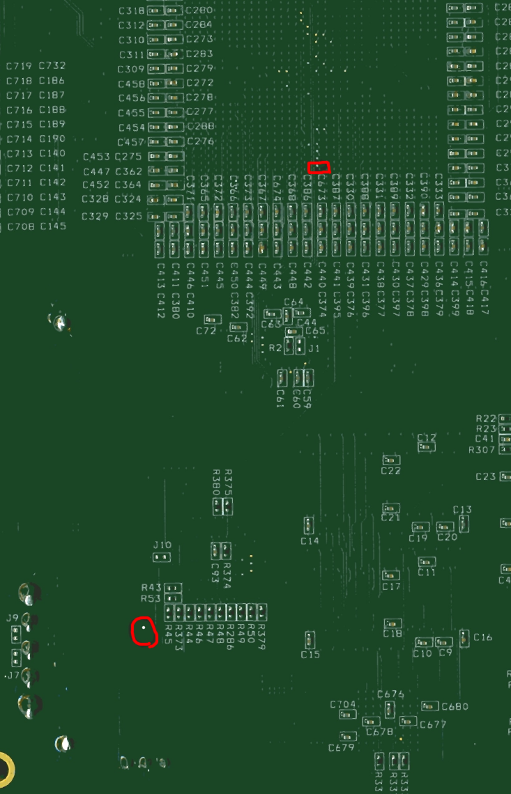
- The white line is the TCK-wire.:
TRB2b and TRB2c
They need a patch for the JTAG communication to work reliably. A 50 Ohm resistor in series with the TCK line coming from the ETRAX will do the job. So the line has to be cut and a 50Ohm resistor has to bridge the gap. Here are the pictures for that: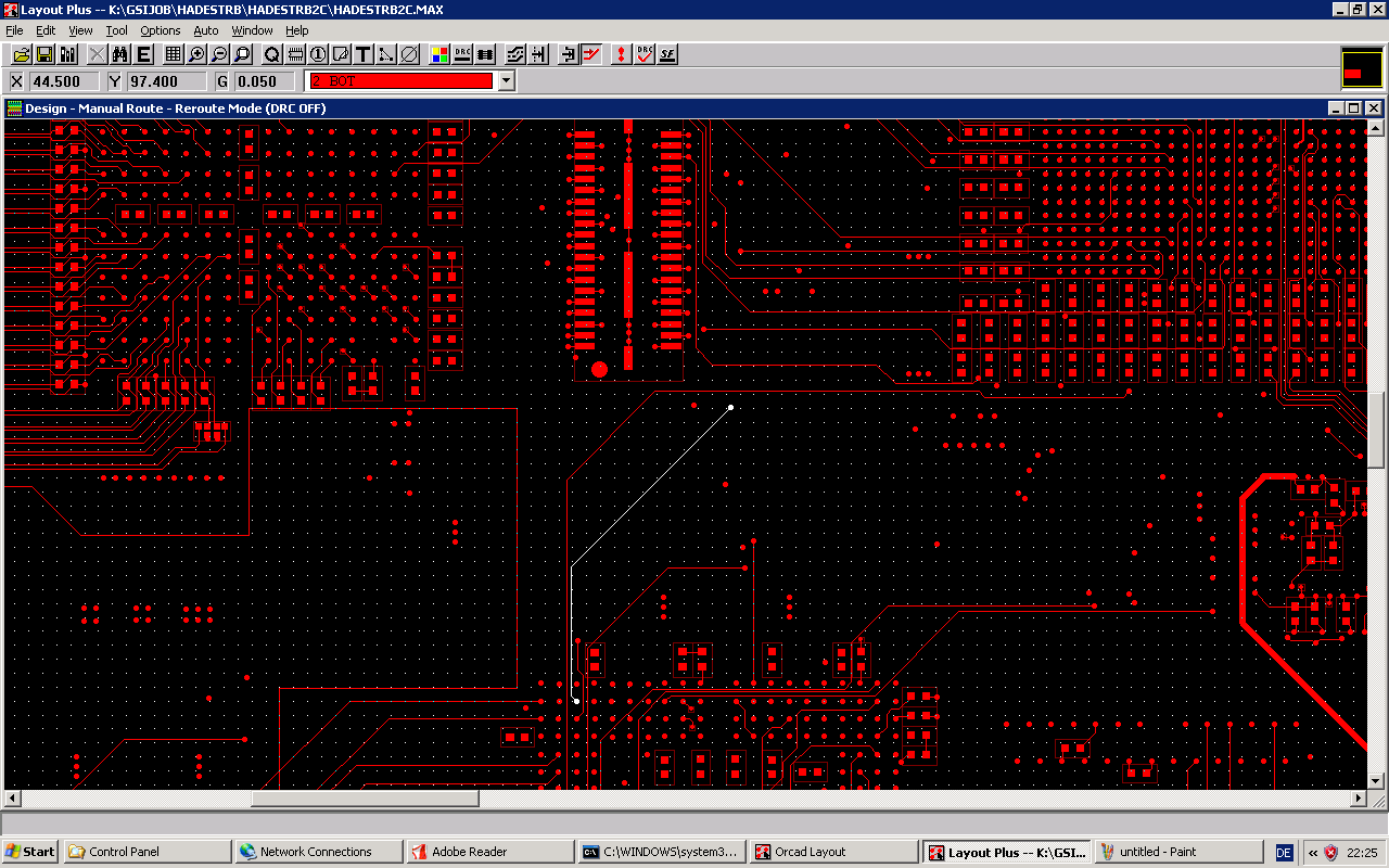
Hub2
Connect Temperature Sensor to FPGA1: FPGA-pin H1(lower left pin with testpad) to Pin 80 of AddOn-Connector JTRB2.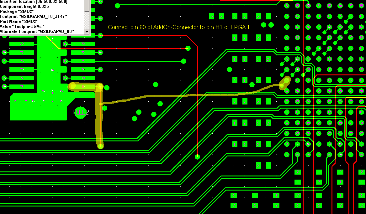
MDC Optical AddOn
Connect Temperature Sensor to FPGA2: FPGA2-Pin AD1 / JT32 (rightmost pad in a group of six) to Via under sensor (right one in row of four).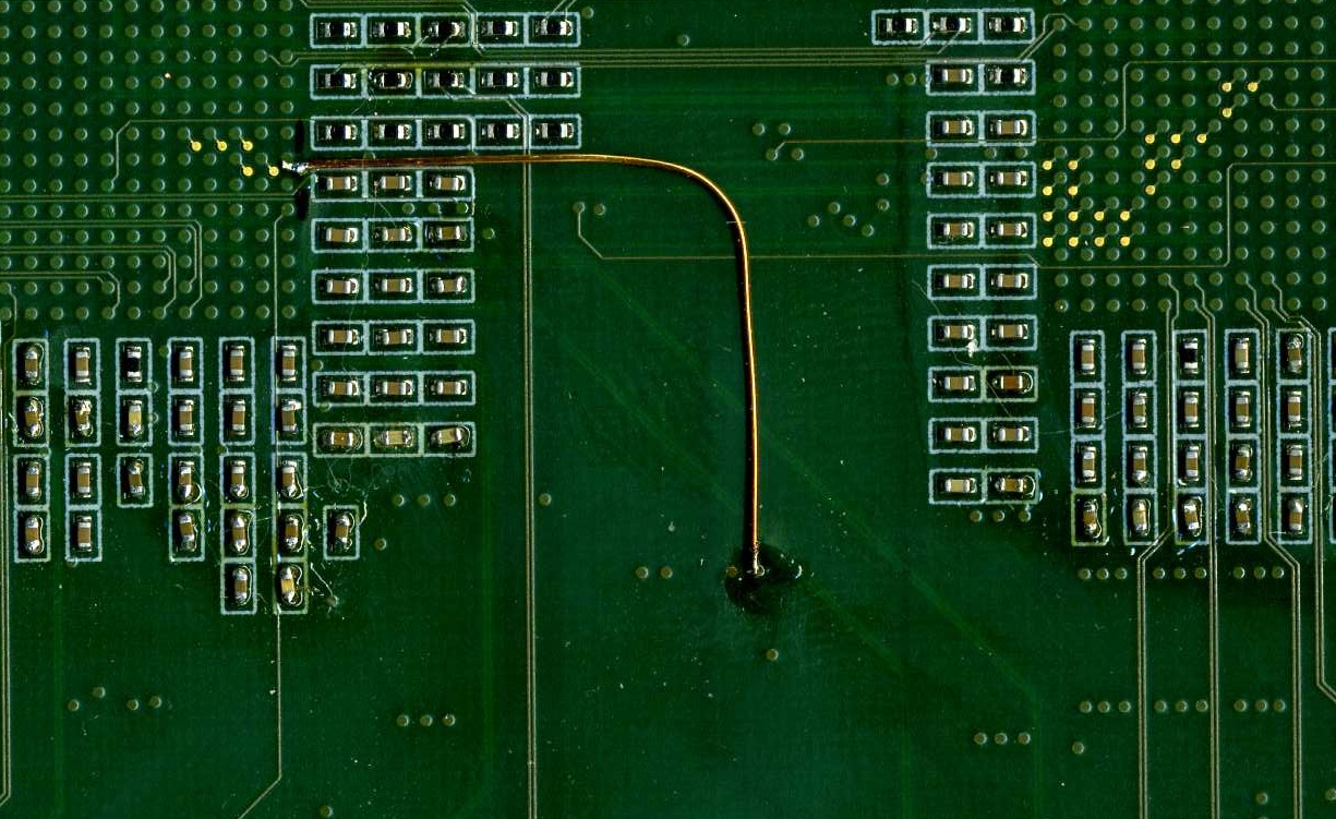 -- JanMichel - 26 Mar 2009
TOF AddOn
No connection on SCK and CS signals between DAC groups and lost connection between UD17 SDO to UD1 SDI. Needed patches (example, because it is enough to connect pin 7 and 8 between groups):UD1 pin 7 -> UD2 pin 7
UD1 pin 8 -> UD2 pin 8
UD5 pin 7 -> UD6 pin 7
UD5 pin 8 -> UD6 pin 8
UD9 pin 7 -> UD10 pin 7
UD9 pin 8 -> UD10 pin 8
UD13 pin 7 -> UD14 pin 7
UD13 pin 8 -> UD14 pin 8


| I | Attachment | Action | Size | Date | Who | Comment |
|---|---|---|---|---|---|---|
| |
MDC_OPTICAL_ADDON001.jpg | manage | 382 K | 2009-03-27 - 11:02 | JanMichel | MDC Optical AddOn: temperature sensor patch |
| |
hub2.png | manage | 31 K | 2009-03-23 - 11:58 | JanMichel | Hub2 Patch: Temperature Sensor to FPGA1 |
| |
trb2b.png | manage | 1 MB | 2009-03-26 - 18:45 | JanMichel | Trb2_B Temperature sensor patch |
| |
trb2c.png | manage | 680 K | 2009-03-26 - 18:44 | JanMichel | Trb2_C temperature sensor patch |
| |
trb_v2c_jtag_patch.png | manage | 77 K | 2009-06-08 - 15:34 | MichaelTraxler | The white line is the TCK-wire. |
Edit | Attach | Print version | History: r8 < r7 < r6 < r5 | Backlinks | View wiki text | Edit wiki text | More topic actions
Topic revision: r8 - 2009-10-27, JanMichel
Copyright © by the contributing authors. All material on this collaboration platform is the property of the contributing authors.
Ideas, requests, problems regarding Foswiki Send feedback | Imprint | Privacy Policy (in German)
Ideas, requests, problems regarding Foswiki Send feedback | Imprint | Privacy Policy (in German)