|
|
You are here: Foswiki>DaqSlowControl Web>HadesDaqDocumentation>VHDLCodeInformation>VHDLConstraints (2009-02-17, MichaelBoehmer)Edit Attach
Information on using VHDL Constraints
Lattice constraints
Constraints for Lattice FPGAs should be located in a separate LPF file, especially if these constraints are PCB related.I/O constraints
IMPORTANT: check your design PAD report that all pins of your design have been correctly assigned to the PCB defined pin positions! You can spend literally hours in debugging just to find out that one signal was not constrained to a pin and has been automatically placed by the mapper to some wrong pin. REMARK: assigning LVDS25 ouptput to "emulated" LVDS pins will lead to an error message, while assigning LVDS25E to any pin pair in a warning - even if the pin pair used can only support LVDS25E. This is a known "feature" of the DRC. Don't follow the recommandation given with the warning to replace the LVDS25E by LVDS25 I/O type, as this will make your design fail with an error! Signals from the top entity of a VHDL design should be located (i.e. fixed to a certain I/O pin) and defined regardings the I/O standard used. This is up to the board designer!LOCATE COMP "CLK100M" SITE "AJ14" ; IOBUF PORT "CLK100M" IO_TYPE=LVDS25 ;This constraint locates the signal "CLK100M" to pin "AJ14", and ensures that a 2.5V LVDS input buffer is being used. Please note that for differential signals only the "true" pin is located, the "complementary" pin is automatically assigned by the mapper.
LOCATE COMP "ADC1_CLK" SITE "F6" ;
IOBUF PORT "ADC1_CLK" IO_TYPE=LVTTL33 PULLMODE=NONE DRIVE=4 SLEWRATE=SLOW;
This output signal is assigned to pin "F6", uses a LowVoltage driver with 3.3V power supply, has no pulldown/pullup resistor enabled, limits the driver capability to 4mA and limits the output driver to "slow" operation (to avoid excessive ringing). In general it is a good idea to limit typical onboard connections in both slewrate and driver capability if possible. The more pins are being used with "SLEWRATE=FAST", and the higher the maximum output current is, the more ground bounce will arise. To avoid long and unreadable LPF files one can also define groups and assign properties to all members of this group:
# LED drivers
LOCATE COMP "FPGA_LED_ADC_0" SITE "AE8" ;
LOCATE COMP "FPGA_LED_ADC_1" SITE "H10" ;
LOCATE COMP "FPGA_LED_6" SITE "G28" ;
LOCATE COMP "FPGA_LED_5" SITE "G27" ;
LOCATE COMP "FPGA_LED_4" SITE "H28" ;
LOCATE COMP "FPGA_LED_3" SITE "H27" ;
LOCATE COMP "FPGA_LED_RXD" SITE "J28" ;
LOCATE COMP "FPGA_LED_TXD" SITE "J27" ;
LOCATE COMP "FPGA_LED_LINK" SITE "K26" ;

DEFINE PORT GROUP "led_output_group" "FPGA_LED*" ;
IOBUF GROUP "led_output_group" IO_TYPE=LVTTL33 PULLMODE=NONE DRIVE=16 SLEWRATE=SLOW ;
Just be careful and choose your wildcards correctly.
Timing constraints
IMPORTANT: no clock inside your design must be without a timing constraint. This is not a guideline, but a rule. Without this vital information MAP and PAR will not known the maximum allowed delay between register outputs and register inputs. REMARK: The Lattice software will for some reasons accept the "true" signal names as defined in your VHDL code for NET based constraints, but complain about not being able to find signals afterwards. Anyhow, the constraints are taken over from "true" signal names to the PAR given ones. I recommend to stick to the "true" names (like SYSCLK), even if the PAR report will show some other fancy name (like SYSCLK_0)... REMARK2: huge Lattice FPGA (ECP2M-100) offer you plenty of logic, and plenty of routing delays. Unconstrained designs from smaller devices (like the ECP2M-35) which worked fine on the small device will very likely fail on the huge device, as routing delays between logic will consume up to 80% of your allowable delay, and the placer will distribute the components of your design widely around the fabric center. REMARK3: timing constraints alone won't help in all cases. If you have small dedicated clock domains with high frequency clocks, the placer will not be able to solve it on its own. You will need some placement constraints (see below). RECOMMANDATION: using clear and unique clock net names (like "clk100m") allows easy wildcard usage for frequency constraints.# DLL 100MHz -> 100MHz LOCATE COMP "THE_100M_DLL/dll_100m_0_0" SITE "DLL_R103C1" ; FREQUENCY NET "sysclk" 100.000000 MHz ; USE PRIMARY PURE NET "sysclk" QUADRANT_BL QUADRANT_BR QUADRANT_TL QUADRANT_TR ;This constraint forces a DLL to a fixed place inside the Lattice FPGA fabric (please note that the RxxCxx name varies with the chip used, and is not documentated by Lattice, you have to look up this information inside the floorplaner by hand - have fun). The frequency of the DLL output clock is set to 100MHz, leaving 10ns of routing between register stages. This clock is used in all parts inside the fabric, so it is assigned to be used in all quadrants of the FPGA clocking scheme as primary clock net, without using the DCS feature.
# PLL ADC0: 240MHz -> 240MHz/40MHz
LOCATE COMP "THE_ADC0_HANDLER/PLL_240M/PLLDINST_0" SITE "SPLL_R67C1" ;
FREQUENCY NET "THE_ADC0_HANDLER/clk240m" 240.000000 MHz;
FREQUENCY NET "THE_ADC0_HANDLER/clk240m_PHASE" 240.000000 MHz;
FREQUENCY NET "THE_ADC0_HANDLER/clk40m" 40.000000 MHz;
USE PRIMARY PURE NET "THE_ADC0_HANDLER/clk240m" QUADRANT_BL ;
USE PRIMARY PURE NET "THE_ADC0_HANDLER/clk240m_PHASE" QUADRANT_BL ;
USE PRIMARY PURE NET "THE_ADC0_HANDLER/clk40m" QUADRANT_BL ;
This PLL is also forced to a certain ASIC place inside the fabric (which is chosen according the prefered CLKI input pins), but the resulting clock nets are limited to one quadrant of the clock nets (as these clocks are "local"). Don't mix this up with "secondary" clock nets - as the "CLK240M" is used for feeding an ECLK line, it must originate from primary clock net. Next step to take: identify pathes which are not critical for your timing, in this example (RICH ADCM) I take the TRBnet RegIO control register outputs. They set up certain things in my frontend related circuits, and partially cross a clockdomain (especially the general reset signal for all user logic!).
# Relaxed timing constraints for slow control signals (TRBnet -> APV logic)
DEFINE CELL GROUP "slow_ctrl_signals_group" "*regio*buf_REGISTERS_OUT*" ;
MULTICYCLE FROM GROUP "slow_ctrl_signals_group" CLKNET "sysclk" TO CLKNET "clk40m_apv" 2 X ;
Syntax is somehow made: Jan uses "generate" to instantiate the blocks, so the names given to the registers (written and read by TRBnet) are not so clear, and you have to identify them in the post-PAR floorplaner. Watch out: names given here are case sensitive. In the above example I define a CELL group (i.e. registers) by matching their names to "*regio*buf_REGISTERS_OUT*"; you are highly recommened to check the spelling inside the grouping GUI of the floorplaner spreadsheet view. As I use only part of the register outputs in the 40MHz clock domain, and as the rest of them stays within the 100MHz domain, I narrow the selection by specifying the source and destination clock domain (sysclk = 100MHz). This means: slow control signals from the "slow_ctrl_signals_group" which do not leave the 100MHz clock domain, but stay within, will still be checked for compliance with the 100MHz timing constraint. The "2 X" relaxation will yield in 30ns being allowed for the delay at maximum; please check the TN1018 from Lattice for the calculation method, which is not straight forward (i.e. it is NOT simply 2x 10ns = 20ns).
Placement constraints
The placer is stupid. Period. And the bigger the FPGA fabric gets, the more stupid it will act. Next period. As an example for the need of placement constraints I take the ADS5271 ADC interface, which takes eight serial DDR data streams, one reference clock (ADCLK) and one DDR bitclock (LCLK). The ADC gets 40MHz clock as sampling clock, and returns a 6x LCLK (240MHz), one word clock (40MHz), and DDR data streams to be converted into parallel data again. The LCLK is fed into a SPLL, a phase shifted version is fed back into the ECLK (to adjust timing on the PCB, if necessary), and the normal 240MHz SPLL output is fed into the fabric for data handling. This part is covered by mainly timing constraints and PLL placement. Each ADC channel is handled by IDDR registers in the IO block of the ECP2M, together with some shift registers and a bit ordering multiplexer. This part runs at 240MHz, and is controlled by an entity which samples the ADCLK and generates some control signals for concenating the shift register contents into a parallel 12bit data word in the right bit order. If you don't take constrain the placement, all logic needed for handing the ADC will be distributed around the fabric center, far far away from the I/O registers, leading to timing failures due to the large fabric routing pathes. Solution:- define a GROUP for each design entity (i.e. one group for each channel, one group for the timing control)
- take a look into the flor planner, and define regions near the I/O to get the logic placed into
- do it the Xilinx way (XAPP774) and instantiate four copies of the timing circuit, one inbetween two ADC channel, to keep routing short
architecture behaviour of adc_ser2par is

-- Placer Directives
attribute HGROUP : string;
-- for whole architecture
attribute HGROUP of behaviour : architecture  is "ADC_SER2PAR_group";
Each instantiation will be handled now as a single GROUP. Next, we need some REGION definitions inside the fabric (LPF file):
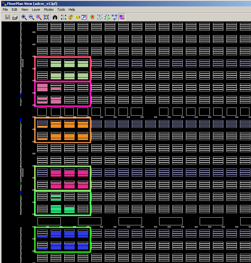
REGION "ADC0_0_SER2PAR" "R99C2" 2 4 ;
UGROUP "THE_ADC0_HANDLER/THE_ADC_SER2PAR_0/ADC_SER2PAR_group" BLKNAME THE_ADC0_HANDLER/THE_ADC_SER2PAR_0 ;
LOCATE UGROUP "THE_ADC0_HANDLER/THE_ADC_SER2PAR_0/ADC_SER2PAR_group" REGION "ADC0_0_SER2PAR" ;
REGION "ADC0_1_SER2PAR" "R95C2" 2 4 ;
UGROUP "THE_ADC0_HANDLER/THE_ADC_SER2PAR_1/ADC_SER2PAR_group" BLKNAME THE_ADC0_HANDLER/THE_ADC_SER2PAR_1 ;
LOCATE UGROUP "THE_ADC0_HANDLER/THE_ADC_SER2PAR_1/ADC_SER2PAR_group" REGION "ADC0_1_SER2PAR" ;
Note: first a region is defined, with an anchor (RxxCyy denotes row and column), width and height. The HGROUP inside the VHDL file (note the reference by instantiation name) is converted into a UGROUP (don't ask me, I took this over myself from some other source), and then the group is placed inside the REGION. Important note: take care to include all needed logic inside the target region. If you need EBRs, include them in the region, otherwise placement will fail. Also take care: the fabric structure is irregular. Some rows have distributed RAM facilities, some don't, and some rows are not LFUs, but EBRs or MULTs. You will need the floor planer for this task. The result will be like this, where the boxes show the regions, and the colored LFUs used logic space:
 Next thing to watch out: you need to prevent the smart software from optimizing the four instantiations of the timing circuit into a single one, as this will lead to routing delays for the control signals too big for fulfilling the constraints.
So additional constraints are needed which attach to the instantiations:
Next thing to watch out: you need to prevent the smart software from optimizing the four instantiations of the timing circuit into a single one, as this will lead to routing delays for the control signals too big for fulfilling the constraints.
So additional constraints are needed which attach to the instantiations:
   -- Use the force... to keep all four timing circuits in
    attribute syn_noprune : boolean;
    attribute syn_noprune of THE_ADC_DEMUX_0 : label is true;
    attribute syn_noprune of THE_ADC_DEMUX_1 : label is true;
    attribute syn_noprune of THE_ADC_DEMUX_2 : label is true;
    attribute syn_noprune of THE_ADC_DEMUX_3 : label is true;

   -- Use the force... to keep all four timing circuits in
    attribute noclip : string;
    attribute noclip of THE_ADC_DEMUX_0 : label is "1";
    attribute noclip of THE_ADC_DEMUX_1 : label is "1";
    attribute noclip of THE_ADC_DEMUX_2 : label is "1";
    attribute noclip of THE_ADC_DEMUX_3 : label is "1";
Please note: the NOCLIP attribute affects the Lattice software, the NOPRUNE attribute the SynplifyPro.
To be continued...
-- MichaelBoehmer - 16 Feb 2009Xilinx constraints
I/O constraints
For each I/O pin used the location at the fpga must be given (in most cases you don't have to care about this, because other people did before)NET "LVDS_IN<15>" LOC = "j6";
If there are signals with a frequency of more than 150MHz, the standard mode of the outputs is too slow, thus you have to select fast slew rate mode:
NET "LVDS_OUT<0>" LOC = "c21" | SLEW="FAST";
Timing Constraints
You have to state how fast the clock is you want to use. If you don't do this, the effort of the place and route process might be to weak to get usable results:NET "CLK_IN" TNM_NET = CLK_IN_GRP; TIMESPEC "TS_DDR_IN" = PERIOD CLK_IN_GRP 10 ns HIGH 50 %;
Do not specify faster clock signals than they are actually. This might be good to optimize internal logic paths but causes problems when constraining external data buses since the I/O net delays dominate all other delays and are sometimes even longer than one clock period.
An external data bus needs some constraints as well. You should state, during which part of a clock cycle the data is valid and can be read. In this case the data will be available two nanoseconds before the rising edge of the clock and will be hold until two nanoseconds after the rising edge:
INST "DATA_IN<*>" TNM = "IN_DATA"; TIMEGRP "IN_DATA" OFFSET = IN 2 ns VALID 4 BEFORE "CLK_IN"
For general information on offset constraints read Xilinx White Paper WP237.
Dual Data rate constraints
When using dual data rate outputs (what can easily be done using the Xilinx FDDR primitives) one has to constrain both edges of the clock, for example:#the external clock for ddr NET "DDR_CLK_IN" TNM_NET = DDR_IN_CLK_GRP; TIMESPEC "TS_DDR_IN" = PERIOD DDR_IN_CLK_GRP 10 ns HIGH 50 %; #the i/o pads used for DDR INST "DDR_IN<*>" TNM = "IN_DDR"; INST "DDR_OUT<*>" TNM = "OUT_DDR"; #select flipflops working with falling and rising edge INST "DDR_IN_rising_FF<*>" TNM = "rising_ffs"; INST "DDR_IN_falling_FF<*>" TNM = "falling_ffs"; #specify the timing at the pads of the chip TIMEGRP "IN_DDR" OFFSET = IN 1 ns VALID 3 BEFORE "DDR_CLK_IN" TIMEGRP "rising_ffs"; #offset for falling edge is shifted by -PERIOD/2 TIMEGRP "IN_DDR" OFFSET = IN -4 ns VALID 3 BEFORE "DDR_CLK_IN" TIMEGRP "falling_ffs"; #timing for the outputs TIMEGRP "OUT_DDR" OFFSET = OUT 10 ns AFTER "CLK";Choosing the output offset as short as possible forces the toolchain to optimize all signals, resulting in only little skew on the output ports. See Xilinx Answer Record 12819 for some more information. On slow synchronous interfaces you can simply shift the clock by ninety degrees to guarantee that the data is available when it is read. On fast interfaces one has to take the routing delays into account. This may even result in a shift backwards! On xilinx devices, the clock can be shifted by as little as (Clockperiod/255) using a DCM.
General Information about constraints
* TimingConstraintsGuide6i_7i_8i.pdf: Very useful information about constraints. -- JanMichel - 03 Jul 2007Edit | Attach | Print version | History: r7 < r6 < r5 < r4 | Backlinks | View wiki text | Edit wiki text | More topic actions
Topic revision: r7 - 2009-02-17, MichaelBoehmer
Copyright © by the contributing authors. All material on this collaboration platform is the property of the contributing authors.
Ideas, requests, problems regarding Foswiki Send feedback | Imprint | Privacy Policy (in German)
Ideas, requests, problems regarding Foswiki Send feedback | Imprint | Privacy Policy (in German)